TSMC adds $100 billion to Arizona buildout after Q2 beat
TSMC plans at least four more Arizona facilities as AI-related chip demand lifts revenue and prompts a higher 2026 capex plan.
By Dominic Okoye · Staff Writer
· 3 min read
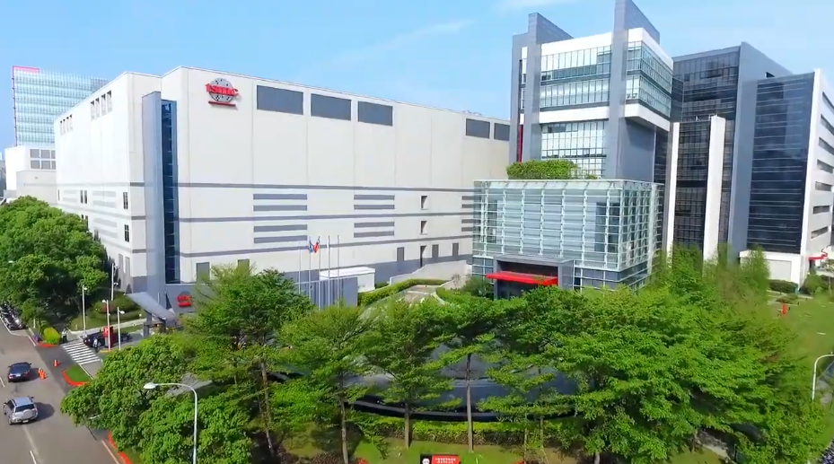
Taiwan Semiconductor Manufacturing Co. said it will put another $100 billion into its Arizona manufacturing complex, taking the planned investment in the site to $265 billion, after reporting second-quarter results above analyst expectations. The new spending covers at least four additional facilities, a larger U.S. footprint for the foundry at a time when advanced AI and data center chips are driving its growth.
TSMC reported second-quarter profit of 706.56 billion New Taiwan dollars, about $21.89 billion, up 77% from a year earlier. Analysts had expected NT$632.64 billion. Revenue rose 36% year over year to $39.45 billion, slightly ahead of consensus estimates, according to the company.
The mix of that revenue matters more than the beat. TSMC said roughly two-thirds of sales came from its high-performance computing unit, which includes data center chips. That business grew 20% from the prior quarter, making it the fastest-growing part of the company’s core operations. Smartphone chip sales, still TSMC’s second-largest revenue stream, fell 4%.
Arizona shifts toward leading-edge nodes
Two of the four planned Arizona facilities will manufacture chips using processes in the two-nanometer class and below, TSMC said. Those plants will sit alongside another N2 fab in Arizona that the company began building last year.
The Arizona expansion is therefore tied less to generic capacity and more to the most advanced part of TSMC’s roadmap. The company said technologies at seven nanometers and below accounted for 77% of wafer revenue in the quarter. Its five-nanometer process remained the largest contributor, with 33% of sales. The newer N2 process, introduced last year, represented 2% of revenue.
TSMC describes N2 as its first process to use gate-all-around transistors, a design intended to improve power efficiency and give chip designers more flexibility than prior transistor architectures. The node also uses metal-insulator-metal capacitors, or MIM capacitors, to help manage electrical flow inside chips.
The company is building variants of the two-nanometer process for different end markets. It has outlined N2X for data center chips, a version that consumes more power than the standard process while aiming for higher performance. In April, TSMC introduced N2A for automotive applications.
Packaging capacity joins the fab plan
The other two new Arizona plants will produce advanced packaging components, according to TSMC. The company did not say which packaging technologies will be made there.
That omission is notable because packaging has become a constraint for high-end AI processors that combine multiple dies and high-bandwidth memory. TSMC’s portfolio includes SoIC, which stacks chiplets vertically, and CoWoS, which places dies side by side on a shared substrate. Earlier this year, the company previewed a CoWoS upgrade designed to connect 10 large compute dies with 20 HBM stacks.
TSMC also raised its spending plan for 2026. The company now expects capital expenditures of $60 billion to $64 billion, up from a previous forecast of $52 billion to $56 billion. It also lifted its full-year revenue growth outlook to a little more than 40%.
The company’s roadmap extends beyond N2. TSMC plans to launch a 1.6-nanometer process next year that moves power delivery circuitry beneath transistors to improve efficiency. It has also named two later processes, A14 and A12, though it did not provide additional financial detail for those nodes in the announcement.
This story draws on original reporting from SiliconANGLE.