Intel puts ASML High NA EUV tools into chip production
ASML says Intel is using its TwinScan EXE lithography systems on selected Intel 18A layers as ASML raises its 2026 revenue outlook.
By Wei-Lin Zhao · AI Correspondent
· 3 min read
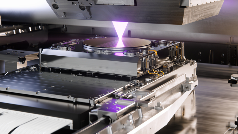
Intel has begun producing processors with ASML’s TwinScan EXE High NA EUV lithography systems, ASML said July 15, moving the newest class of chipmaking exposure tools into an Intel manufacturing flow. No purchase price for the systems, production volume or customer shipments tied to the High NA EUV steps were disclosed, but the development is material for Intel’s foundry ambitions and for ASML’s next lithography platform.
ASML disclosed the milestone alongside second-quarter results that beat analyst expectations. The Dutch equipment supplier reported 9.3 billion euros in sales for the quarter ended June 28, above the 8.8 billion euros analysts expected, according to CNBC. Net profit was 2.9 billion euros, also above consensus.
Lithography systems pattern transistor features onto silicon wafers. ASML is the dominant supplier of the most advanced systems used by leading-edge chip manufacturers, and its EUV tools have become a gating item for companies trying to push process technology forward.
The new detail is Intel’s use of ASML’s EXE series, the company’s High NA EUV platform, for selected layers in Intel 18A. ASML said Intel is using the tools to manufacture some layers in the process, but the companies did not specify which layers, how many steps are involved or what yield levels Intel has reached.
High NA moves from installation to production
ASML’s EXE machines use a higher numerical aperture than the prior generation of EUV tools. The company says the EXE platform has a 51% higher NA than its predecessor and can print patterns at eight-nanometer resolution, compared with 13-nanometer patterns available before the EXE series.
That matters because smaller patterned features are one of the ways chipmakers improve performance and power efficiency. In practice, advanced processors are built from many layers, and fabs typically reserve the most expensive lithography equipment for the layers where tighter patterning is needed most, while using less advanced tools elsewhere.
Intel installed an EXE:5000 system at its Hillsboro, Oregon, site two years ago. It later added a more capable EXE:5200B and completed acceptance testing for that system in December, according to ASML.
ASML said both machines generate laser light by vaporizing tiny drops of lead. The EXE:5200B adds upgraded optical components, which ASML says improve throughput and patterning accuracy compared with the earlier EXE:5000.
Intel is using the EXE-based line to mass produce a subset of its Intel Core Ultra Series 3 laptop processors, according to ASML. The highest-end chips in that family include a 12-core CPU, a 12-core GPU and an AI accelerator. Intel did not disclose how much of the product line depends on High NA EUV steps.
Naga Chandrasekaran, executive vice president and general manager of Intel Foundry, said Intel has qualified High NA EUV on selected Intel 18A product layers and is using its current tool fleet to increase output while developing options for future nodes. The statement did not include yield, cost or capacity figures.
ASML lifts its outlook
ASML also raised its full-year revenue forecast to a range of 43 billion to 45 billion euros. The top end of that range is 5 billion euros higher than the company’s prior outlook.
The company said it expects demand for its equipment to remain strong in the second half of the year. ASML also plans to increase manufacturing capacity by 30% in each of the next two years across some production lines.
For Intel, the announcement gives its foundry roadmap a concrete manufacturing proof point at a time when customers and investors are looking for evidence that Intel 18A can move beyond process claims. For ASML, Intel’s use of High NA EUV in production is an early validation signal for a platform that chipmakers will need to justify against high tool costs and complex integration work.
This story draws on original reporting from SiliconANGLE.